Introduction
This experiment is based on an example in Nicolas Collins’ book: “Handmade Electronic Music, The Art of Hardware Hacking”. The motivation for this experiment is to learn IC logic chips and to prepare inexpensive experiments for sound making electronics workshops. This is a first version, please be aware of possible errors. All corrections and contributions for improvement are highly appreciated. This post will be updated.
The misuse of Quad NAND Gate 4093 chip makes simple & cheap way to synthesise modulating square waves. Misuse, since the 4093 chip was not designed to make sounds but to do boolean logic, as a member of highly successful CMOS 4000 series IC chips form late sixties.
A single NAND gate has two inputs and one output. The 4093 chip has four NAND gates, hence the name QuadNAND gate. The NAND stands for one of the common boolean logics (Not AND) where two input states, highs(ones) or lows(zeros), define the state of the output. In NAND case, if neither of inputs are high (being low) the output keeps high. If both of the inputs are pulled high the output inverts to low. If one of the inputs is low the output is always high. The chip uses Scmitt Trigger comparators, which provides noisless & direct swapping of the states.
To turn this to sound it helps to understand basics of the sound. To put it very short, when there is changing states there is frequency. If the frequency oscillates through air and is in the range of hearing, there is sound. If we do the above mentioned state swapping we generate oscillation, a square wave signal of highs and lows, which can be amplified and heard.
Basic square wave can be made with just one NAND gate. The first input is connected high(+5 to 15V) the second is connected low(GND) via capacitor and the output is fed back to the second input via resistor. The chain of events in a fast loop:
- input1 is driven high, the input2 is low, making the output high
- the high output recharges the capacitor in time affected by the feedback resistor
- charged capacitor pulls the input2 high, output goes low, capacitor discharges
- back to the beginning
The frequency generated is based on the capacitance and resistance of the components menitoned above. Increasing the resistance with eg. a potentiometer, less current will flow to capacitor, slowing the “swapping”, lowering the pitch. The higher the capacitance, the longer it takes to recharge, forcing the range of the sweeping pitch lower. This experiment uses 100k pots with 0.1uF and 2.2uF caps. The big cap keep the range very low, in rhythmic clicks, where the small one takes the range high in clear pitch frequencies.
NAND gates can modulate each other. By connecting the output of gate1 to the input1 of gate2, the swapping high-low cycle enables and disables the second gate very fast while the the second gate produces its own frequencies. This can be fed further to the gate3 and so on. This results to complex square wave modulations worth experimenting so read on.

Making it
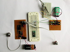
This configuration can be done with breadboard, which is highly recommended for experimenting the logic first. For this first version, I used stripboard and connectors for changing between two caps and inserting variable resistors. Wiring here can be simplified. I have all wires on component side for clarity. This circuit works for me, this explanation is not proofed, build it with your own risk and please report any errors to me.

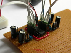
1. Solder the 4093 chip with enough space on the sides. Using socket is always wise. I chanced it here. Old CMOS chips are sensitive to static so be aware. Solder the GND(black) wire to pin7(lower left) and the +V(red) to pin14(top right) notice the chip orientation from the marker on the top. Remember to cut the strips from the solder side between the pins, see 3b.

2. Solder the two caps between input2(pin2) and gnd. Put the smaller cap closer to the chip, break the connection from bigger cap to ground and solder jumper pins over that break. When jumper is connected the bigger cap goes in parallel with the smaller cap, “overriding” the smaller cap and switching the pitch range to very low end. Solder the output1(pin1) to +V. This connection can be replaced with jumper/switch if you want to trigger the synth sound externally. If you use the same stripline for the cap gnd and the pin1, remember to break it on the solder side!

3. Solder the 4way connector (or wires) to the pins2-5, right besides to the chip. This gives us resistor insert points for gates1&2. Wire the output of gate1(pin3) to the input1 of gate2(pin6). Solder the main power pins or battery clip to +V and GND strips on the top. At this point you can try to test the first gate by putting a resistor in the socket between the pins 2&3 and taking signal from pin3 to the tip of the audioplug and commong GND from the board to the sleeve. Notice the warning of using mains connected amp in section 6 below.

3b. Remember to cut the “multiused” strips from the solder side if using stripboard or wire all the necessary connections if using dot-board. (Sorry for the blobby soldering, I’m still struggling with my new leadfree solder.)
At this point you can try to test the first gate by putting a resistor in the socket between the pins 2&3 and taking signal from pin3 to the tip of the audioplug and commong GND from the board to the sleeve. Notice the warning of using mains connected amp in section 6 below.

4. Solder the caps to the gate2, between pin5 and GND, same jumper break as before. Solder the output of gate2(pin4) to the other side to input1 of gate3(pin8).

5. Solder the caps, jumpers and sockets for gates3&4 accordingly. Check the 4093 specsheet for pin order. Solder the header pins to all gate outputs (pins3,4,10,11), the green headers in the image. Notice, these are the signals for the tip of the audio plug to amp. You need to take the common GND from the board to the sleeve of the audio plug.
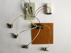
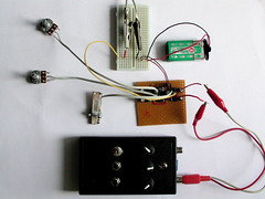
6. Wire the pots / resistors / LDRs to the sockets. Double check the solder points for shorts to strips next to them and use magnifier to check that cutted strips are properly disconnected. Power up the board, feel if the battey or the chip warms up, if so disconnect and look for shorts. Take the audio signal from gate4 output(pin11) to amp together with common GND. Signal is loud, be aware. Caution! Broken amp connected in mains can give an deadly electric shock when using exposed wires. Build simple battery powered amp with LM386 chip like this, or use battery powered active pc speakers if unsure of your amp.
Using it
Start with the first gate, varying the resistance between pins2&3. Take the audio out from header in pin3. Try the difference with a jumper enabling the bigger cap in gate1. Move to gate1 modulating gate2. Put another pot between pins 4&5 and move the audio out signal to pin4 (gate2 output). Experiment with the pots and cap jumpers. Carry on to gate3 and gate4.
Instead of a potentiometer as a controller, you can try different variable resistors. Slider, like mixer fader gives very quick interface of varying the resistance, close to scratching speed. LDR or photoresistor can give gestural control when blocking and revealing light hitting to it.
If you want more automation, you can build the Memory Pot from our earlier examples, where the pot turns are recorded and playdback with variable speeds.
Or you can build simple sequencer varying the resitance in discreet steps like in the SwitchSequencer example below. Check also the videos of our experiments.